We are strongly committed to the development of room temperature gamma ray spectrometers with better energy resolution than currently available from popular scintillation devices. These instruments have important applications in growing areas such as arms control and nonproliferation activities, identification of contraband materials, medical imaging, and radiation protection.
Many of the national laboratories are deeply involved in techniques for the identification and control of special nuclear materials throughout the world. Inspection requirements set by treaties require an increasing level of sophistication and capability in monitoring devices. Our current work with compound semiconductors is aimed largely at this application, and its future development can play an important part in national security issues. A sizable fraction of all the development support currently available at the federal level for radiation instrumentation is currently provided to meet these needs. We expect that this application will remain an important one for the decade ahead. Other work in the area of nanometer-sized detectors has a close tie to the University of Michigan’s Nanotechnology initiative.
While the progress in semiconductor devices has received much attention, recent breakthroughs in scintillators have not gone unnoticed by the international community. Compounds using lanthanum halides have yielded superior energy resolutions in reasonably large sizes, both organic and inorganic scintillators are being developed with particle discrimination in addition to their spectroscopic capabilities.
Flexible, low-cost, high-resolution radiation and optical sensing via nanosemiconductor-based composites.
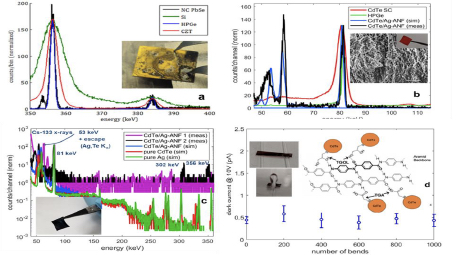
The goal of this project is to use nanocrystalline synthesis to develop a lower-cost, higher-performance semiconductor material based on optoelectronic devices useful in nuclear radiation detection. All existing materials are inadequate for (a) precise, ranged imaging of radioactive sources, or (b) the deployment of low-cost hand-held and portal instruments with negligible false-alarm rates. The primary motivation that drives the development of nanostructured materials, whether nanoscintillators or nanosemiconductors, is that the solution-based fabrication processes can result in an order of magnitude or more reduction in the manufacturing cost, and one may therefore welcome a material that is only slightly worse in performance compared with single-crystalline materials. However, from a fundamental physics perspective, nanostructured materials provide a viable pathway through which transformative improvements in energy resolution can be elicited, because the relative strength of phonon-electron scattering can be quenched. Specifically, one would prefer that W, the energy consumed during the creation of an electron-hole pair be reduced to the bandgap; that is, be limited only by energy conservation. This would result in more charge carriers, which enhances the size of the signal and reduces the statistical counting noise because more of the incident energy is converted into signal carriers. For nuclear radiation detectors, the realization of a uniform multi-exciton response would allow one to tolerate relatively large band-gaps because the uncertainty in the energy determination would then be more dependent on fabrication non-uniformities rather than on signal carrier counting statistics.
Achieving large volumes with reproducible behavior is challenging because compared with solution growth of atomic crystals, the inter-particle potentials between nanoparticles are not exactly matched from batch-to-batch and particle-to-particle. To reduce the sensitivity of the volumetric growth to variations in the particle morphology and charge-state, we used templated growth in the form of polymeric compounds. Specifically, we have prepared free-standing, flexible, and lightweight conductors comprised of semiconducting nanoparticles (NPs) grafted upon a Kevlar-based aramid nanofiber (ANF) matrix, a combination is realized through a simple spin-coating followed by incorporation of the NPs through vacuum filtration. When this process is implemented with semiconducting nanoparticles, such as PbTe or CdTe NPs, the regularized bonding of the nanoparticles along the fiber backbone produces close-packed self-assembly, and a bendable, strong device. Thus, we have demonstrated that colloidal solids and flexible nanosemiconductor-polymer composites can both yield room-temperature energy resolutions comparable to or superior to LN2-cooled HPGe, all through low-cost, easily-scalable solution-based chemical synthesis. Despite this demonstration, the degree to which nanoscale confinement improves the charge conversion efficiency and, potentially, enhances the detection efficiency is not yet fully understood, noting that the intensities of the higher energy peaks (e.g., 302 keV, 356 keV) are higher than expected than that from a bulk sample of equivalent thickness. Our goal in this project is to improve the resolution with which radiation is sensed by several orders of magnitude (closer to the eV level rather than the current keV level). We will demonstrate high-resolution solids of variable flexibility while addressing this limitation on the device end. The same physical mechanism (suppressed phonon-electron scattering) that can quench counting statistical noise can also be used to quench the multiplication noise accrued during avalanche gain.

The first step of the project is focused on describing the underlying physics of the interaction between radiation (γ, neutrons, charge particles) and nanoparticles. This study depends on the ability to make monodispersed nanoparticles of the targeted shape, interconnecting those nanoparticles so that dot-to-dot transport is elicited, and forming sizable sensing volumes so that the charge conversion and transport behavior can be monitored. We mitigate the risk of failure in this regard by examining different pathways to achieving nanostructured sensing solids, particularly with respect to the ligand-chemistry control which sits at the heart of the materials functionalization work. During the research, we plan to focus on the organic synthesis of PbSe and the aqueous synthesis of PbTe and CdTe because they allow one to study the full range of strong-confinement physics, and in the case of PbTe, the compound also provides a high-Z high-density conversion component.
The second step will add the study low-cost fabrication methods by which high-resolution solids have form-factor flexibility and various degrees of pliability. We plan to control the mechanical properties- the strength, the fracture toughness, the flexibility, the extendibility- via the polymeric components in the composite. The knowledge gleaned will be applied to demonstrate high-resolution (< 0.3 %) radiation detection with solids of controlled flexibility and strength. Our goal is to elicit transformational improvements in the resolution, but from a practical standpoint, the noise from existing preamplifiers limits our ability o fully demonstrate the intrinsic resolution of the nanostructured media. The same physical mechanism (suppressed phonon-electron scattering) that can quench counting statistical noise can also be used to quench the multiplication noise accrued during avalanche gain, the degree to which will also be examined. Further work will quantify the limits of efficiency and gain performance for flexible (optical) photonic sensing configurations from the nanosemiconductor composites, and demonstrate the degree to which multi-mode (sensing, stopping, resilient) shielding can be enhanced by using strong-confinement physics.
Understanding the role of valence in bright scintillators
The current generation of scintillator detectors provides optical output at the time the radiation interacts in the detector medium. The output can be proportional to fluence or energy, but the light output ends once the charge kinetics at each site of interaction are complete. Typically, each electron produced through ionization generates at most one detectable photon and the timescale of emission is limited by the relatively slow speed of hole capture at an impurity site. However, we propose to overcome both these limitations with new approaches based on valence control of the scintillating ion.
The current generation of scintillator detectors provides optical output at the time the radiation interacts in the detector medium. The output can be proportional to fluence or energy, but the light output ends once the charge kinetics at each site of interaction are complete. Typically, each electron produced through ionization generates at most one detectable photon and the timescale of emission is limited by the relatively slow speed of hole capture at an impurity site. However, we propose to overcome both these limitations with new approaches based on valence control of the scintillating ion.

To remove the limitation of one signal photon per induced ionization electron, active interrogation with a laser can be used to read out valence-modified atoms created by electron capture following passage of ionizing radiation. In preliminary research, trivalent rare earth ions in CaF2 were reduced to stable divalent ones following ionization of the host by 60Co gamma irradiation. The reduced ions were detected by tuning the wavelength of a readout laser to an optical resonance of the divalent rare earth species. Resonant excitation of the divalent ions resulted in fluorescence at a unique characteristic wavelength. Neither the constituents of the detection medium nor the population of unmodified, trivalent dopant ions were excited in the optical readout process. Hence, this generated an output signal that was proportional to the number of host ionization events but could be integrated over time to improve photon statistics. This approach potentially provides an arbitrarily large signal from each valence change induced by the radiation, limited only by the integration time. Moreover, the detection medium is resettable, returning the divalent species to its original trivalent state, using optical erasure at a different wavelength of incident laser light.

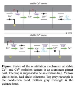
Exploiting Valence-Modified Luminescence to Enhance Scintillator Performance. To speed up and enhance scintillation rates, valence-modified ions can also be added to the detection medium to avoid the slowest step in the emission process. To illustrate how this works we note that in conventional scintillators, using trivalent Ce as an example, the excitation energy comes from electron-hole pairs liberated in the host by ionizing radiation. Scintillation originates from Ce sites, but before light emission can take place, a Ce3+ center must capture a slow-moving hole and then attract an electron to undergo recombination. The rate-limiting step is hole-capture because the effective mass of the hole is much greater than that of the electron. For example, in Gadolinium Gallium Garnet (GGG) which is singly-doped with Ce3+, the scintillation rate is relatively slow due to the slow rate of hole-capture. However, if the crystal is co-doped with Mg, which has a strong preference for divalency, some of the Ce3+ ions convert to Ce4+ to maintain charge neutrality (cf. Fig. reproduced from Ref. 1). The key point to note is that Ce4+ ions can directly undergo recombination by simply capturing the fast-moving electron. There is no need for Ce4+ to capture a hole first to produce scintillation. This is analogous to the single carrier effect that revolutionized room temperature semiconductors, since the limiting step of hole transport is eliminated.
Tailoring of activator valence states for enhancement as well as acceleration of Ce luminescence has been confirmed experimentally in Mg,Ce:GGG2, as well as other scintillators3. However the phenomenology and relevant exploitable materials remain poorly understood. We are currently investigating methods of increasing the proportion of Ce3+ sites occupied by Ce4+ ions in alternate hosts to increase not only the emission rate but also the signal intensity. For example, a specific host of interest is SrCe2O4 which contains Ce3+ ions as part of the stoichiometry and should tolerate high Ce4+ by moving to off-stoichiometric compositions with elevated Sr content (Sr1+xCe2-xO4). A benefit of choosing Strontium is that Sr2+ has an ionic radius slightly larger than that of either Ce3+ or Ce4+. Consequently, the sites available for Sr2+, Ce3+, and Ce4+ are all interchangeable in size, so a high concentration of Ce4+ may be achievable. Spinel and perovskite crystals may also be considered in the search for compositional flexibility to maximize the density of fast Ce4+ recombination sites.
Finally, similar to ionization density effects in organic scintillators, we seek to uncover diagnostic time signatures from scintillator pulses. These have been found to enable particle discrimination in inorganic scintillators4, but more recently have been reputed to enable much higher energy resolution5-6 in conventional materials. Time-resolved luminescence on the nanosecond and sub-nanosecond timescale needed to distinguish between recombination at Ce4+ versus Ce4+ centers as well as to discern time signatures for different particles can readily be performed with time correlation spectroscopy at DYNAMO7 and NERS laser facilities. Michigan has particular strength in such measurements from both its semiconductor and organic scintillator R&D.
References
- Needs, Trends, and Advances in Inorganic Scintillators, C. Dujardi , E. Auffray, E. Bourret-Courchesne, et al., IEEE TRANSACTIONS ON NUCLEAR SCIENCE, VOL. 65, NO. 8, AUGUST 2018.
- Recent R&D Trends in Inorganic Single-Crystal Scintillator Materials for Radiation Detection, M. Nikl and A. Yoshikawa, Adv. Optical Mater. 2015, 3, 463–481.
- Scintillator Design Via Codoping, C. L. MELCHER et al., JPS Conf. Proc., 11, 020001 (2016).
- Large Format Li Co-Doped Nai:Tl (Nailtm) Scintillation Detector For Gamma-Ray And Neutron Dual Detection, P.R. Menge, K. Yang, and V. Ouspenski, Proceedings of the 12th Pacific Rim Conference on Ceramic and Glass Technology: Ceramic Transactions, Volume 264, 2018.
- Gridin, S., Williams, R.T., Belsky, A., Galenin, E., Gektin, A., Shiran, N., Vasiukov, S., Vasil’Ev, A., Carrier Trap Parameters in NaI with Tl, In, and Eu Dopants, (2019) Journal of Physical Chemistry C, 123 (22), pp. 13519-13530.
- 3% energy resolution for NaI(Tl) – from dream to reality. (#2865), A. Gektin, Amcrys, Ltd., Kharkiv, Ukraine, Presented at IEEE NSS 2019, Manchester, U.K., 30 Oct 2019.
- https://dynamo.engin.umich.edu (Accessed 4 November 2019).
Progress Reports
The first year’s progress on this project can be found at:
Upcoming plans for research are here:
